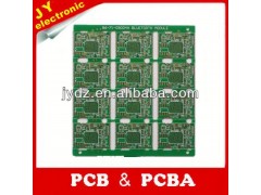
| 原産地: | 中国(本土) | 銘柄: | JY | モデル番号: | 2 layer pcb | Min.線幅: | 0.08mm | 基材: | FR4,FR1,CEM3,Aluminum,Ceramic | 表面の仕上げ: | HASL,Lead Free HASL, OSP,ENIG,Gold | Min.行送り: | 0.08mm | 板厚さ: | 0.5~3.2mm | Min.穴のサイズ: | 0.15mm | 銅の厚さ: | 1oz~4oz | Layer: | 2 layer pcb, double sided pcb | Max. Panel Size: | 541*647mm(Special can do to 950mm) | Finish Hole Size: | PTH +/-0.003 ,NPTH +/-0.002" | Hole Position Accuracy: | +/-0.003" | Ring annulus: | Min 0.1mm | Aspect Ratio: | Min 1:8 | Solder Mask Rrgistration: | +/-0.003" | Layer to layer Rrgistration: | +/-0.003" | Copper Feature to Holes Rrgistration: | +/-0.003" | Company product: | 2 layer pcb, double side pcb |
包装
| 包装: | Nnerのパッキング: 真空packing/ポリ袋の外のパッキング: 標準的なカートンのパッキング |
仕様
fme pcb connectors
Double layer pcb is our hot sale product.
You make a good choice! 

Welcome to Dalian JY Electronic Technology Co., Ltd.
There is professional pcb&pcba design group waiting for you! Also there is pcb&pcba factory producing for you! Welcome your inquiry!
![]()
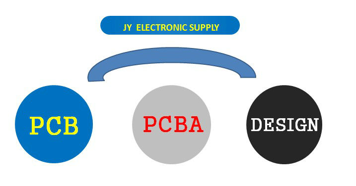


We independently research and develop Internet control system, Internet numericalcontrol system, robot control system and produce hardware and software independently for control management etc.. Also supply clients SAS Marketing Automation. Door bell, car alarm, mobile solar charger design by us is most welcome products.
PCB Certificates Details
![]()
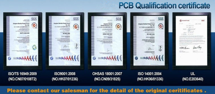
All our certificates are just for PCB, not for PCBA, pls notice.
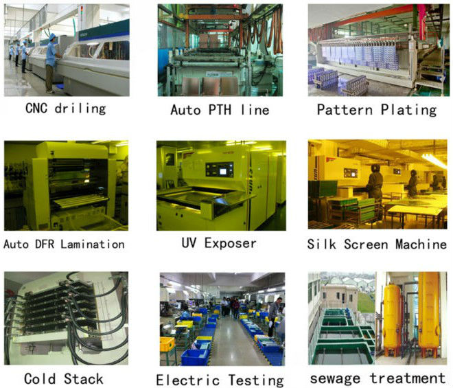
JY Factory Real Photos

![]()

The last three pieces photos are pcba factory.
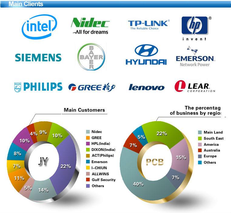
JY Main Clients

JY PCB Engineering Capacity
| No. | Item | Spec |
| 1 | Layers | 1 to 24 layers |
| 2 | Max working panel area | 457 x 610 mm |
| 3 | Min board thickness | 4 layer: 0.40mm |
| 6 layer: 0.80mm | ||
| 8 layer: 1.00mm | ||
| 10 layer: 1.20mm | ||
| 4 | Min trace width | 0.10mm |
| 5 | Min spacing | 0.10mm |
| 6 | Min hole diameter | 0.20mm |
| 7 | Min Copper thickness in hole | 0.020mm |
| 8 | PTH size tolerance | ±0.05mm |
| 9 | NPTH size tolerance | ±0.025mm |
| 10 | Hole position tolerance | ±0.05mm |
| 11 | Dimension tolerance | ±0.1mm |
| 12 | Min solder mask dam | 0.08mm |
| 13 | Insulation resistance | 1E+12Ω (normal condition) |
| 14 | Max Board thickness/Hole size Rate | '10:1 |
| 15 | Thermal shock endurance | 288 3 times in 10sec |
| 16 | Max Board twist and wrap | ≤0.7% |
| 17 | High Vlotage endurance | 1.3KV/mm |
| 18 | Copper foil peel off endurance | 1.4N/mm |
| 19 | Hardness of resist ink | ≥6H |
| 20 | Flame resistance | 94V-0 |
| 21 | Impedance control | ±5% |
| 22 | Certificate | ISO 9001:2000;ISO 14001;ISO/TS16949:2002 ,UL E203640 |
JY PCB QC System


JY PCB Payment way and Delivery way.
Our payment way is flexible and multiple. For samll quantity order, we supply Express delivery.For mass order,we delivery by ship.
fme pcb connectors


Purchase Tips:
A.For PCB order, please provide Gerber file or pcb file. Any detail is also welcomed if no gerber file.
B.Large PCB quantity order, quotation will be based on SQM.
C.For PCBA order, please provide the Gerber file, pcb file and BOM List.
D.Reverse engineering and PCB clone service can be supplied with your PCB sample.
E.Any question, welcome to contact our sales person Lucy Gao by sending inquries, your satisfactionis our pleasure.

